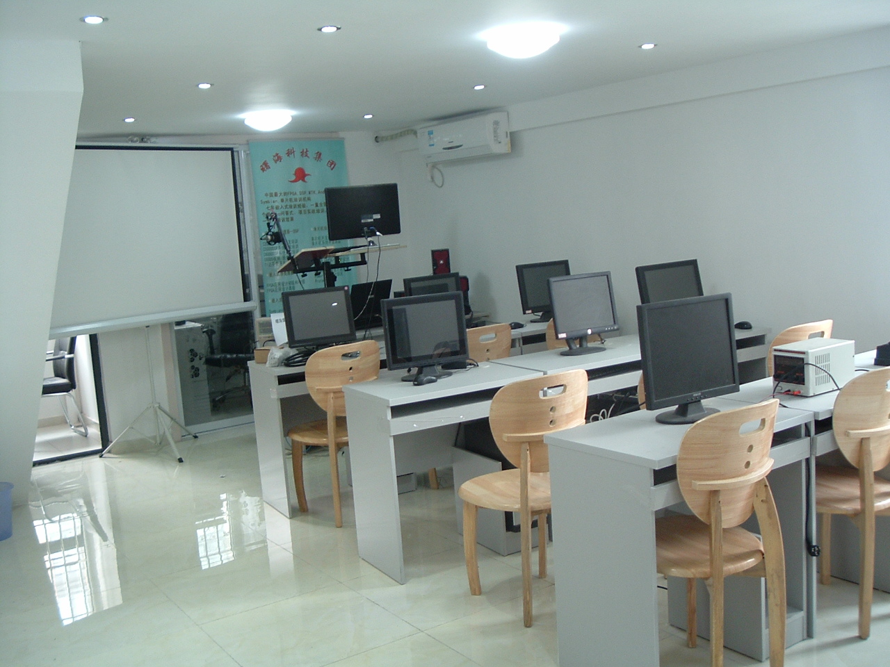
培训方式以讲课和实验穿插进行
课程描述:
第一阶段 Design Compiler 1
Overview
This course covers the ASIC synthesis flow using Design Compiler Topographical / Graphical -- from reading in an RTL design (Verilog, SystemVerilog and VHDL) to generating a final gate-level netlist. You will learn how to read in your design file(s), specify your libraries and physical data, constrain a complex design for timing and floorplan, apply synthesis techniques using Ultra, compile to achieve timing closure and an acceptable congestion, analyze the synthesis results for timing and congestion, and generate output data that works with downstream layout tools.
You will verify the logic equivalence of synthesis transformations (such as Datapath optimizations and Register Retiming) to that of an RTL design using Formality. The course includes labs to reinforce and practice key topics discussed in lecture. All the covered commands and flows are printed separately in a 5-page Job Aid, which you can refer to back at work.
- Objectives
- At the end of this workshop the student should be able to:
- Create a setup file to specify the libraries and physical data
- Read in a hierarchical design
- Constrain a complex design for timing, taking into account different environmental attributes such as output loading, input drive strength, process, voltage and temperature variations, as well as post-layout effects such as clock skew
- Constrain multiple (generated) clocks considering Signal integrity analysis
- Execute the recommended synthesis techniques to achieve timing closure
- Analyze and Improve global route congestion
- Perform test-ready synthesis
- Verify the logic equivalence of a synthesized netlist compared to an RTL design
- Write DC-Tcl scripts to constrain designs, and run synthesis
- Generate and interpret timing, constraint, and other debugging reports
- Understand the effect that RTL coding style can have on synthesis results
- Generate output data (netlist, constraints, scan-def) that works with downstream physical design or layout tools
Course Outline
- Unit 1
- Introduction to Synthesis
- Design and Technology Data
- Design and Library Objects
- Timing Constraints
- Unit 2
- Environmental Attributes
- Synthesis Optimization Techniques
- Timing Analysis
- Unit 3
- Additional Constraint Options
- Multiple Clocks and Timing Exceptions
- Congestion Analysis and Optimization
- Post-Synthesis Output Data
- Conclusion
第二阶段 Design Compiler 2: Low Power
Overview
At the end of this one day, seminar based, workshop you will understand how to apply both traditional and UPF based power optimization techniques during RTL synthesis and scan insertion:
For single voltage designs, you will learn how to apply the 2 traditional power optimization techniques of clock gating and leakage power recovery, optimizing for dynamic power and leakage power respectively.
For multi-voltage or multi-supply designs, you will learn how to apply the IEEE 1801 UPF flow that uses a power intent specification which is applied to RTL designs. You will understand how to synthesize RTL designs for the required power intent and power-optimization requirements using top-down vs. hierarchical UPF methodologies. You will also learn how to insert scan chains to the synthesized netlist ensure that the gate level design does not have any multi-voltage violations, before writing out design data for Place and Route.
- Objectives
At the end of this workshop the student should be able to:
- Apply clock gating to a design at the RTL and gate level
- Perform multi-stage, hierarchical, and power driven clock gating
- Perform leakage optimization using multi Vt libraries
- Restrict the usage of leaky cells
- Specify power intent using UPF
- Demonstrate flexible isolation strategy in UPF 2.0
- Check for UPF readiness of library, reporting PG pins
- State the purpose of SCMR attribute in library
- Recognize tradeoff when using dual vs. single rail special cells
- Correctly specify PVT requirements
- State how the 6 special cells are synthesized
- Describe supply net aware Always on Synthesis
- Apply 2 key debugging commands in a UPF flow
- Control voltage, power domain mixing when inserting scan chains
- Allow/prevent the reuse of level shifters and isolation cells between scan and functional paths
- Minimize toggle in functional logic during scan shifting
- Validate SCANDEF information for place and route
Course Outline
- Clock Gating
- Leakage Power Optimization
- Power Intent using IEEE 1801 UPF
- Library Requirements
- Synthesis with UPF
- Power Aware DFT
第三阶段 DFT Compiler
Overview
In this workshop you will learn to use DFT Compiler to perform RTL and gate-level DFT rule checks, fix DFT DRC rule violations, and to insert scan using top-down and bottom-up flows. The workshop explores essential techniques to support large, multi-million gate SOC designs including the bottom-up scan insertion flow in the logical (Design Compiler) domain. Techniques learned include: performing scan insertion in a top-down flow; meeting scan requirements for number of scan chains, maximum chain length and reusing functional pins for scan testing, inserting an On-Chip Clocking (OCC) controller for At-Speed testing using internal clocks; and using Adaptive Scan (DFTMAX) to insert additional DFT hardware to reduce the test time and the test data volume required for a given fault coverage.
- Objectives
- At the end of this workshop the student should be able to:
- Create a test protocol for a design and customize the initialization sequence, if needed, to prepare for DFT DRC checks
- Perform DFT DRC checks at the RTL, pre-DFT, and post-DFT stages
- Recognize common design constructs that cause typical DFT violations
- Automatically correct certain DFT violations at the gate level using AutoFix
- Implement top-down scan insertion flow achieving well-balanced scan chains
- Write a script to perform all the steps in the DFT flow, including exporting all the required files for ATPG and Place & Route
- Develop a bottom-up scan insertion script for full gate-level designs to use Test Models at the top-level to improve capacity and runtime
- Insert an On-Chip Clocking (OCC) controller to use for At-Speed testing with internal clocks
- Modify a scan insertion script to include DFT-MAX Adaptive Scan compression
Course Outline
- Unit 1
- Introduction to Scan Testing
- DFT Compiler Flows and Setup
- Test Protocol
- DFT Design Rule Checks
- Unit 2
- DFT DRC GUI Debug
- DRC Fixing
- Top-Down Scan Insertion
- Exporting Files
- Unit 3
- High Capacity DFT Flows
- On-Chip Clocking (OCC)
- Multi-Mode DFT
- DFT MAX


 shuhaipeixun
 1299983702
 总部李老师
总部李老师